- Offer Profile
-
As a leading provider of laser manufacturing solutions, LPKF Laser & Electronics helps to create more powerful electronic systems and increase functionality and efficiency for a broad range of applications and industries.
LPKF is a leading supplier of laser-based solutions for the technology industry. Our laser systems are vital in the manufacture of printed circuit boards, microchips, automotive parts, solar panels and many other components.
Our machines allow our customers to manufacture smaller and higher- precision components. At the same time, the functionality of the components can be increased and new design options can be used. This creates products on the cutting edge of technology, both for the industry and for consumers.
Electronics Manufacturing
- As a highly specialized photonics machinery manufacturer and the world's leading provider of laser-driven production processes, LPKF Laser & Electronics offers all-in-one solutions for a broad range of applications.
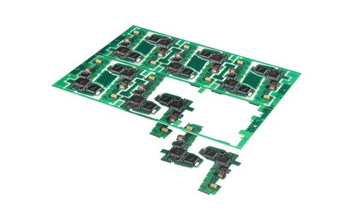
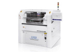
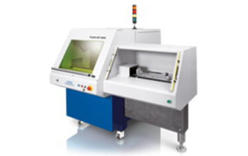
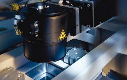
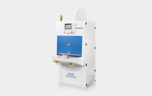
Laser Depaneling for PCBA/EMS
-
Minimize stress, maximize yield: stress free cutting of populated rigid and flexible PCBs
- CleanCut technology
- Automated handling
- New LPKF PicoLine laser systems
Stress-free, clean cutting of populated rigid and flexible PCBs
Circuit reliability is significantly improved and fewer or even no extra cleaning processes are required with laser cutting, which thus offers significant cost savings for laser depaneling. A new family of depaneling systems delivers an unprecedented combination of performance, reliability, and low cost.
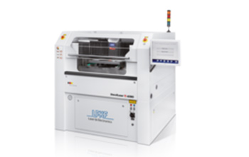
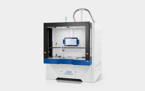
Laser Drilling and Cutting for PCB Shops
-
Stress free cutting and drilling of rigid PCBs, FPCBs and coverlays.
- CleanCut technology
- Short-pulse systems
- New LPKF PicoLine systems
Stress-free processing of rigid PCBs, FPCBs and coverlays
With easy handling, a small footprint and short changeover times LPKF laser systems offer best-in-class solutions to help customers compete in today's on-demand world. The laser allows for maximum use of the base material and production time.
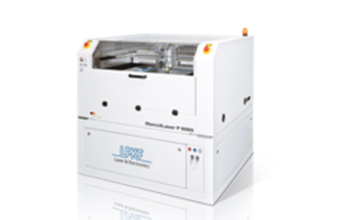
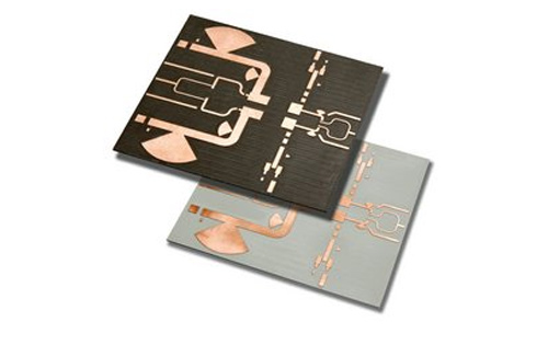
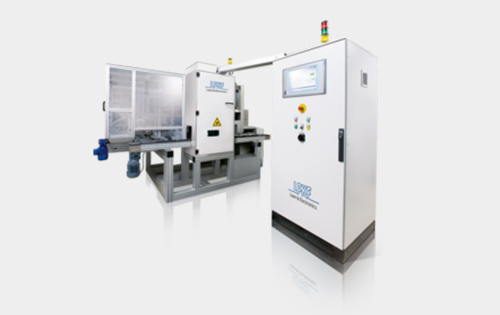
SMT Stencils and Micro-cut Parts
-
LPKF StencilLasers, the first choice for SMT stencil manufacturers: Exact geometries for each and every stencil aperture.
- Step stencils
- XXL stencils
- Micro-cut parts made from thin metal foils
New dimensions in precision laser cutting
Innovative variants of the high-end LPKF StencilLaser G 6080 laser system set new benchmarks in two dimensions: Extremely small openings of the highest quality enable new stencil applications and micro-cut parts can be manufactured with the highest precision from stainless steel sheets up to a thickness of 4 mm.
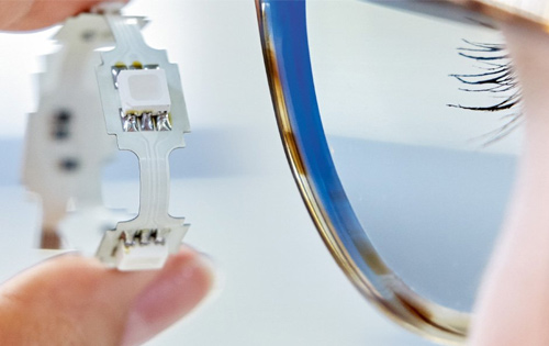
IC Packaging
-
Incorporate higher IC functionality -- Processing of mold compounds
- Through mold vias (TMVs),
- Singulation of IC packages,
- Through glass vias (TGVs)
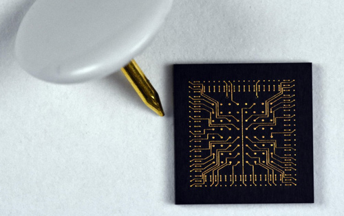
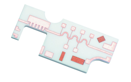
3D-MID With Laser Direct Structuring (LDS)
- Mechatronic integrated devices (MIDs) enable greater miniaturization. Laser-based structuring technologies are being increasingly used for manufacturing innovative mechatronic systems and microsystems such as sensors and actuators.
Electronics Manufacturing Products
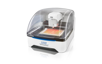
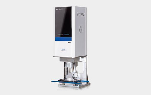
Vitrion S 5000
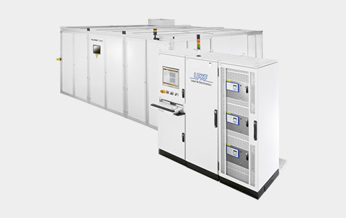
- LIDE production system for processing glass wafers for future packaging and semiconductor applications.
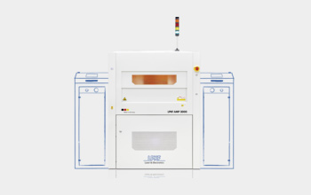
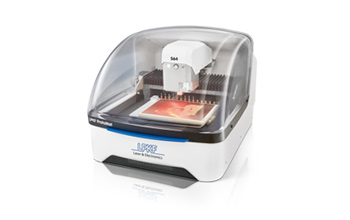
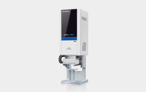
AMP 3000
- The laser system for the AMP technology to electrically functionalize the real-estate of the Epoxy Mold Compound.
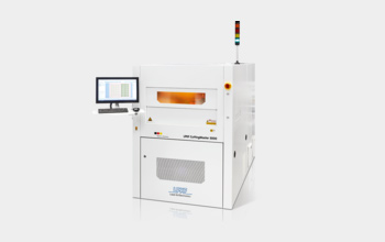
CuttingMaster 3000
- The most precise laser depaneling systems with a large working area of 500 mm x 350 mm.
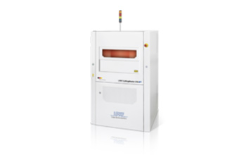
CuttingMaster 2000
- Compact and extremely cost-efficient: Flexibility, space saving, design freedom - depaneling by laser opens up numerous potentials.
MicroCut 6080
- The new benchmark for extremely small apertures in stencil sheets.
PowerCut 6080
- Cuts thick metal sheets - up to 4 mm (150 mil) - with micrometer accuracy.
StencilLaser G 6080
- The most productive and fastest cutting system for SMT stencils.
StencilLaser P 6060
- The LPKF StencilLaser P 6060 is a state-of-the-art laser system for the production of SMT stencils.
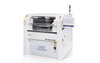
PicoLine 5000
- High-performance laser systems equipped with a large working area, CleanCut Technology and short-pulse technology. Variants for automated handling are available.
MicroLine 2000
- Compact, cost-efficient and inline-capable - cut printed circuit boards and panels with UV lasers.
MicroLine 5000
- The MicroLine 5000 is a cost-efficient laser drilling and cutting system with a large working area, specifically tailored to the needs of the PCB industry. The system is suitable for the singulation of IC Compounds.
Fusion3D 1100
- The LPKF Fusion3D 1100 laser structuring system is a cost-effective entry into the 3D circuit market.
Fusion3D 1200
- Equipped with a high-quality rotary indexing table, small, medium and large series of 3D circuit carriers can be produced particularly economically.
Fusion3D 1500
- The LPKF Fusion3D 1500 combines the power of LPKF's high-performance structuring machines with the flexibility of a compact system.
Research & in-house PCB prototyping
-
Shaping the future of technology
In the development of new products, fast iterations are required. The machines and equipment from LPKF Laser & Electronics give you all the possible options for PCB prototyping and micro material processing. Find out all about the systems and processes with which LPKF helps its customers succeed.
In-house production of printed circuit board prototypes
In the development of new products, the time factor is critical. Security of in-house data also plays a major role. From idea to mass-produced goods in minimal time with in-house rapid PCB prototyping. Develop a printed circuit board, manufacture it in just one day, and keep all data in-house: can this be done even faster and more securely?
Micro material processing
Development of electronic components has been progressing at an astounding pace for years. Integrated circuits are becoming more compact, and at the same time clock speeds are increasing. High frequencies, steep rising edges, and minimal space place huge demands on the printed circuit board. The response has been to use new substrate materials, which are much more difficult to process than the standard FR4 material is. Laser systems from LPKF Laser & Electronics are universal tools for micro material processing, but they can do much more than just machine substrates for printed circuit boards!

Why in-house PCB prototyping?
-
Easy to use, efficient, reliable
LPKF's benchtop PCB prototyping systems provide the ideal in-house research and development solution for virtually any engineering environment. Every LPKF ProtoMat® is built to be the best of its class, with thousands of the individually calibrated systems installed world-wide. It's no surprise to hear LPKF customers explain that their ProtoMat® system is the most important tool in the R&D lab.
Prototyping with LPKF ProtoMat systems
LPKF Laser & Electronics' benchtop prototyping systems produce high-performance boards that match or exceed the quality of outsourced PCB prototypes. With an LPKF ProtoMat® PCB milling machine, prototype PCBs can be made and tested within a single day - without the use of hazardous and messy chemical etching tanks. Any problems with the initial design can be identified early, allowing for revisions 2 & 3 to be completed in the same day!
Micro material processing in the lab
-
On the right track to innovation.
Innovation and experience
A key advantage of the laser as a tool is the small focal spot size of the laser beam. Thus, in the extreme case, cut channels with widths of just 15 µm can be produced. This precision also applies, e.g., to corner radii and sharp cut edges – making the laser particularly interesting for HF applications.
Large bandwidth
The range of options available with LPKF ProtoLasers comprises:
- Cold ablation of various thin films with picosecond lasers.Use of ultrashort pulses opens up completely new possibilities in material processing. The pulse width is so short that virtually no thermal effects arise in the vicinity of the point of impingement on the material. The ProtoLaser R4 is hence suitable, e.g., for machining delicate layers for OLED lighting or complex thin-film solar cells.
- Gentle machining of laminated materials such as FR4 boards with lasers in the “green” range of the visible light spectrum. The ProtoLaser S4 is predestined for surface machining of PCB materials.
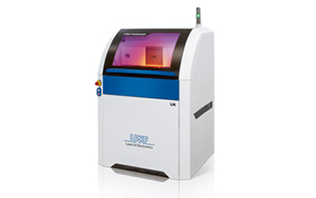
- Precise machining of ceramics. The ProtoLaser U4, which is equipped with a UV laser source, structures, e.g., metal layers on ceramic substrates (Al2O3), can score ceramics, and is outstanding for processing of LTCCs (structuring, cutting, and drilling).
Process steps for prototyping
-
Coordinated methods and tools from a single source
From structuring of the base material to complex production-level multilayers the entire prototyping process -- design, production, testing and optimization -- can be completed in a single day.
From layout data to fully functional PCB
LPKF offers easy-to-use, compatible solutions for all process steps.
Software with intuitive operation
-
Step by step through data preperation and the manufacturing process
The LPKF circuit board plotters and ProtoLasers come with the powerful system software CircuitPro. It imports the data from the design software, uses it to generate the individual processing steps, prepares it for production, and guides the user through each step of the manufacturing process.
PCB structuring
-
Generate conductive traces within minutes using mechanical systems and laser processes.
The faster way to create circuit boards
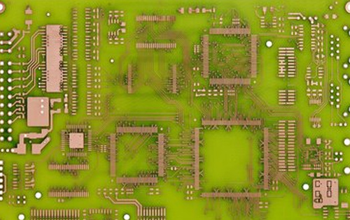
Mechanical or laser systems enable single-sided and double-sided PCBs, multilayers, high-capacity circuits, RF and microwave PCBs, and rigid and flex PCBs to be manufactured – thus offering exciting options for electronic products.
Milling the conductor pattern
1- & 2-sided PCBs and multilayers
Mechanical and laser systems selectively remove the copper layers on single- and double-sided circuit boards, thereby creating insulating channels that precisely delineate the required conductive traces and pads. The circuit board plotters also drill all the necessary holes in the boards.
PCB drilling
-
Produce through-holes and blind vias
All holes on a circuit board can be drilled using LPKF circuit board plotters or LPKF ProtoLasers.
Laser drilling
Laser processing is an efficient technology for producing drilled microvias with diameters of less than 200 μm.. LPKF ProtoLaser systems can be used for processing of a wide variety of board substrates, e.g., RCC, FR4 and FR5, Teflon®, and Thermount®.
Our application specialists would be happy to help you with the sampling of your materials.
Mechanical drilling
For drilling of FR4 boards with different shapes, resolutions, and densities, LPKF circuit board plotters represent an efficient, low-cost solution. Drill holes with diameters starting at 0.15 mm. LPKF ProtoLaser series laser systems are available if you require even smaller diameters. Our application specialists would be happy to advise you on which technology is suitable for your application.

Through-hole plating processes
-
Work with no chemicals and by electroplating - Fast, reliable, laboratory-compatible
The prototyping process isn’t finished after the circuit board has been manufactured. With the subsequent processes – through-hole plating, solder mask coating, solder paste printing, assembly, and reflow soldering – a circuit board becomes an electronic assembly.
Two paths to the perfect results
- The chemical-free through-hole plating process LPKF ProConduct® metallizes through-holes with diameters of up to 0.4 mm and aspect ratios of up to 1:4. At 19 milliohms on average, the electrical resistance of the plated-through holes is extremely low.
For through-hole electroplating, the LPKF Contac S4 combines various electrolytic and chemical processes in a compact safety housing.
- The chemical-free through-hole plating process LPKF ProConduct® metallizes through-holes with diameters of up to 0.4 mm and aspect ratios of up to 1:4. At 19 milliohms on average, the electrical resistance of the plated-through holes is extremely low.
PCB depaneling - cutting
-
Depaneling of PCBs for a wide variety of materials
Depending on the requirements profiles, basically one of two production variants can be selected: mechanical structuring by means of milling or laser structuring. A cutting contour can be implemented in a few minutes.
Easy and flexible
Detaching of the printed circuit boards from the base material is a task that is performed by the LPKF ProtoMats or ProtoLasers. One or more boards are arranged on a base material and separated using a milling tool or an LPKF ProtoLaser. An extensive parameter/tool library delivers the settings for the most important materials. Creation of panels is also optimally supported by the LPKF software.
SMT / Finishing
-
Assembly of PCB prototypes and low volumes
From application of the solder paste to placement of individual components, low-cost and proven processes lead to an electrically functional product in just a few steps.
SMT technology for developers
In series production, surface mount devices (SMDs) are assembled with SMT pick and place machines. Before this process takes place, paste is printed onto the pads on the board. After the SMDs have been placed on the printed circuit board, reflow soldering is performed. All processes and methods used in SMT production – adapted to the requirements of the electronics laboratory – are also available for in-house PCB prototyping.
Multilayers
-
Production of up to eight layers in-house
LPKF offers a complete prototyping product line for production of multilayers in an in-house lab. The multilayers are produced in three simple steps: structuring, lamination, and through-hole plating.
A printed circuit board composed of several layers
A multilayer is made up of multiple layers that are laminated together to form a printed circuit board. The outer layersof a multilayer are usually single-sided PCBs, whereas the inner layers are double-sided materials. Insulating layers, so-called prepregs,are inserted between the conductive layers. Up to four layers can be through-hole plated in a chemical-free process. For electrical connection of up to eight layers through-hole electroplating is recommended.
Research & in-house PCB prototyping Products
ProtoMat S104
- Specialist for RF and microwave applications, fully equipped for the electronics laboratory.
ProtoMat S64
- Allrounder for Rapid PCB Prototyping. The basic system for almost all in-house PCB prototyping applications.
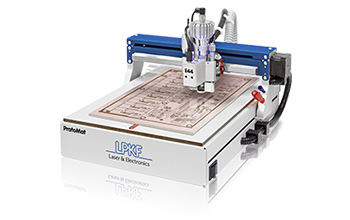
ProtoMat E44
- The cost-effective entry into the world of professional in-house PCB prototyping.
ProtoLaser ST
- The laser table system achieves exact geometries on almost any material and is ideal for structuring single or double-sided printed circuit boards.
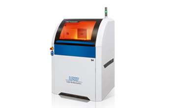
ProtoLaser R4
- Short laser pulses -- gentle material processing. Infinite possibilities in the research laboratory.
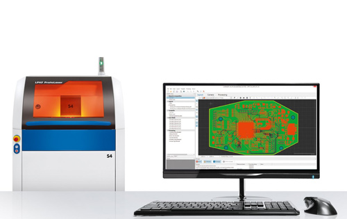
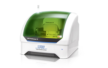
ProtoLaser S4
- The LPKF ProtoLaser S4 is specialized in the structuring of laminated circuit boards.
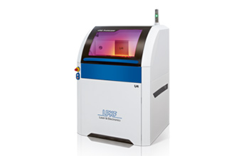
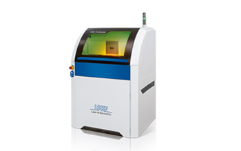
ProtoLaser U4
- UV laser system with a particularly wide range of applications.
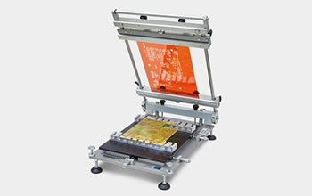
ProtoPrint S4
- Manual SMD fine-pitch stencil printer for precise application of solder paste to circuit boards.
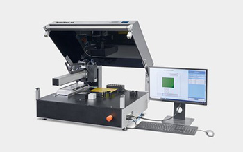
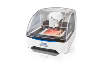
ProtoPlace E4
- Manual pick & place system for SMD assembly of PCB prototypes and small series in the laboratory.
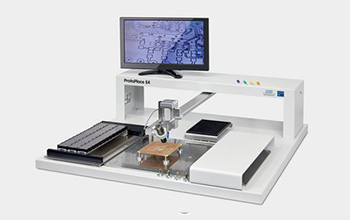
ProtoPlace S4
- Manual pick & place system for SMD assembly of PCB prototypes and small series in the laboratory.
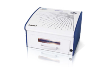
ProtoFlow E
- The LPKF ProtoFlow E is an extremely user-friendly convection oven suitable for SMD soldering.
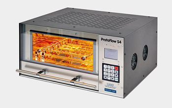
ProtoFlow S4
- Compact reflow oven both for RoHS-compliant lead-free reflow soldering.
ProMask / ProLegend
- In-house system for the application of solder resist masks and legend printing.
Contac S4
- The LPKF Contac S4 provides a reliable electroplating process for through-hole plating.
ProConduct
- LPKF ProConduct is a chemical-free through-hole plating system.
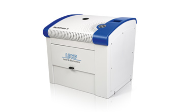
MultiPress S
- The MultiPress S multilayer press presses multilayer circuits made of rigid, rigid-flex and flexible printed circuit board materials.
ProtoLaser
- Structuring of the finest conductor path patterns.
LPKF ProtoMats
- Design and manufacturing of PCB prototypes in just one day.
Laser Plastic Welding

-
Enhancing your production´s efficiency - High-end laser plastic welding with the expert
Joining plastic components in a way that is precise, reliable, and permanent – without adverse chemical, thermal, mechanical effects on the surrounding material? This is a simple job for LPKF laser welding machines!
When it comes to joining plastic components, laser technology has gained an excellent reputation. It efficiently creates plastic joints of unrivaled quality and cost-effectiveness. LPKF has many years of experience and is a global leader in this area.
8 advantages of laser plastic welding with LPKF
- Simple process setup - (nearly) child's play
- Efficient processing in seconds
- Highly flexible processing thanks to easy job setup
- Reliability through process monitoring
- Top quality standards
- Best possible welding results
- Highly available, low-maintenance machines
- On request: Sample
8 benefits of the technology
- New and one-of-a-kind: Identical and repeatable results on all calibrated LPKF laser welding machines
- Perfectly clean: no released particles, no solvents no chemical treatment, no surface damage
- No mechanical stress in the component; joints are even possible close to electronic
- As solid as the material itself: joints that hold
- Precise results: exact weld seams inside components
- Truly impermeable: up to protection class 67
- Aesthetically appealing results
- Flexible and with online process monitoring
Precise welding process
- Precision is achieved by the accurately focused laser beam.
Exact weld seams
- High production reliability for a weld seam density that is visually and functionally outstanding.
Process reliability
- All machine components satisfy the high demands that you also have for your products.
Laser Plastic Welding Products
PowerWeld 3D 8000
-
Innovative technology in the LPKF PowerWeld3D 8000 ensures high performance and quality when welding large 3D plastic parts
Laser Welding of Large 3D Plastic Components
LPKF PowerWeld 3D 8000 with integrated quality control
Innovative technology in the LPKF PowerWeld3D 8000 ensures high performance and quality. Impressive details: This welding system flexibly copes with height differences of up to 400 mm and controls the welding process with integrated joining path monitoring. Short cycle times and a stable process predestine the system for applications in the automotive industry, for example. Components welded with PowerWeld 3D 8000 meet the requirements of protection class IP67.
PowerWeld 2000/2600
-
LPKF PowerWeld 2000/2600: Compact welding system for (almost) every application
Flexible and universal
LPKF PowerWeld 2000/2600: Compact welding system for (almost) every application
The LPKF PowerWeld 2000 and PowerWeld 2600 systems enable high design flexibility. All components are accommodated in the compact housing: laser, control unit and cooling system. The PowerWeld 2600 also features a rotary index table for higher throughput. Integrated online process monitoring ensures optimum workpiece quality and productivity.
PowerWeld 6600
-
LPKF PowerWeld 6600 for economical series production of large components
High-Speed Laser Welding
LPKF PowerWeld 6600 for economical series production of large components
Modern technology for the leading joining technology in the production of medium and large series. - LPKF PowerWeld 6600 for integration into higher-level production control systems.
InlineWeld 9000
-
Everything is possible in laser plastic welding with LPKF: from the combination of individual machine elements to complex robot islands.
The Perfect Machine for Special Requirements
LPKF InlineWeld 9000: A multitude of variants for (nearly) all applications
From our experience with standardized systems we draw creativity for the realization of the most diverse production processes. For customer-specific tasks we combine various features: laser, beam guidance and control, setup of manual assembly workstations, automatic feeding of individual parts... We realize your specific solution up to the complex, automated robotic island.
TMG 3
-
Material qualification by transmission measurement. Calibrated measuring device for the transparency properties of plastics. Ensures the quality of welding and end product.
THE Reference for Transmittance Measurement
Quality inspection prior to laser processing
The transmittance properties of two plastic joining partners are decisive for the quality in laser transmission welding. Checking the material properties before laser plastic welding pays off as part of comprehensive quality assurance system. The TMG 3 is a certified measuring instrument that has been traceably calibrated with the cooperation of the Fraunhofer Institute for Silicate Research ISC.
InlineWeld 2000
-
Laser welding system for economical and reliable joining of cylindrical workpieces. For integration into the automated production line.
Optimal joining of cylindrical components
LPKF InlineWeld 2000: A solution for every requirement
Radial welding of rotationally symmetrical plastic components has never been easier than with the new LPKF InlineWeld 2000, a system developed for automated production lines. Powerful, fast and flexible.
InlineWeld 6200
-
The efficiency miracle: Universal InlineWeld 6200 system for different component and batch sizes. Simple process setup and process monitoring strengthen the efficient use of the system in all industries.
The integrable general-purpose talent
LPKF InlineWeld 6200: Power for smaller components in large lines
The efficiency miracle: Compact inline laser welding system for smaller components and various batch sizes. The universally applicable InlineWeld 6200 enables the economical production of plastic components.
InlineWeld 6600
-
Economical integration system for large quantities in fully automated 24/7 production.
Laser plastic welding system for today and tomorrow
Fully automated production with LPKF InlineWeld 6600
Highest process reliability, greatest possible flexibility and economy: A dream both for developers of plastic components to be joined, and for users in production.
TwinWeld 3D 6000
-
LPKF-patented hybrid welding enables high-quality and virtually stress-free welds in the visible area with extremely flexible contour guidance, even for complex 3D applications.
LPKF TwinWeld 3D 6000
Efficient LPKF hybrid welding on a rotary index table
The LPKF TwinWeld 3D 6000 is equipped with a processing field measuring 600 x 600 x 600 mm for the reliable welding of large plastic components. It also has a rotary index table for improved cycle times.
Photovoltaics
-
Highly efficient and cost-effective laser processing of thin-film modules
Our Allegro systems are unmatched in terms of throughput, availability and accuracy in the market. We are constantly developing these laser scribing systems further. Being a supplier to the most advanced thin-film technologies drives and pushes us to constantly improve our systems with regard to throughput and accuracy as well and being equally important for manufacturer in terms of system uptime. One major part of maintaining uptime is our well organized 24/7 service support in the countries where production takes place.
LPKF Allegro Series: 24/7-production systems
-
Next generation technology delivers greater profits
LPKF Allegro laser scribers
In musical terminology, Allegro means fast. LPKF SolarQuipment’s state-of-the-art laser scribers carry this name due to their outstanding throughput and precision. Imagine a solar module factory to be a great orchestra. The Allegro scribers would be world class players perfectly contributing to the overall goal, lowest cost per Wpeak in production.
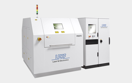
LPKF Presto: R&D and lab system
-
Pure flexibility for labs and R&D
The LPKF Presto is a multifunction scribing tool for laboratory purposes. It allows process development for scribing thin film coatings for CdTe, CIGS and others, as well as the parameter determination for production systems.
LPKF - Thing-Film Laser Scribing
-
Your partner from R&D to high-volume production
We offer solutions for the photovoltaic market
LPKF SolarQuipment GmbH is the technology leader for thin-film module laser scribing equipment. Excellent product quality as well as comprehensive know-how and experience make us an international eligible partner for many well-known thin-film manufacturers. We support our customers from R&D via commissioning of laser scribing equipment in large module manufacturing plants to maintaining high availability in production.
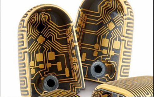
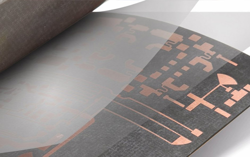
Active Mold Packaging (AMP)
-
Why Active Mold Packaging (AMP)?
To functionalize the real-estate of the epoxy mold compound.
Active Mold Packaging is an easy, time-saving and reliable 2.5D packaging approach, which establishes electrical circuitry on the surface and in the volume of the Epoxy Mold Compound. 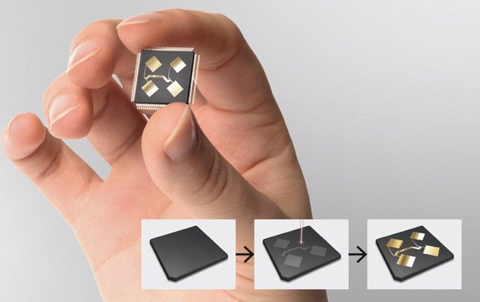
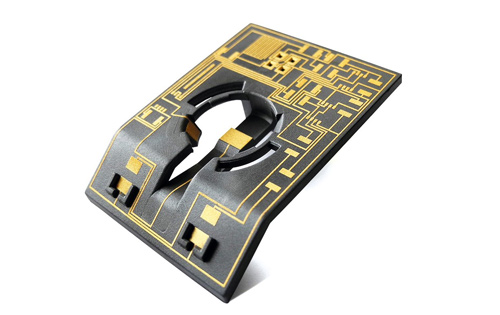
The Active Mold Packaging (AMP) technology
-
Electrically functionalizing the real-estate of the Epoxy Mold Compound.
AMP converts the passive Epoxy Mold Compound (EMC) only used for protection today, into an active carrier of electrical functionality.
AMP stands for Active Mold Packaging
AMP establishes horizontal and vertical interconnect access between active and passive components in a heterogenous 2.5D packaging approach.AMP is based on 3 proven and standardized, electronics manufacturing technologies.
- Molding
Transfer- & Compression-Molding of thermo-set epoxy mold compound, doped with a laser-activateable additive. - Laser Direct Structuring
Laser Direct Structuring and Drilling of the mold compound, activates the additive in the mold compound. - Electro-less plating
Electro-less plating deposits a conformal copper layer on only the laser activated areas of the compound.
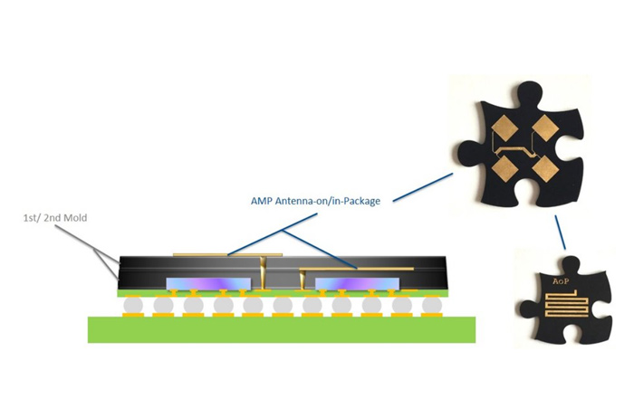
mmWave-Antenna
-
Package and SiP based planar antennas
Active Mold Packaging presents a much simplified and reliable approach to package integrated planar antennas.
RF applications are manifold and demanding. They are used through-out many different industries from consumer electronics to industry, automotive as well as in the air and space sector.
Active Mold Packaging (AMP) is capable of integrating planar antennas in and on the package. While stamp metal or flex antennas can be mounted on top of a package, the twist, AMP is offering, is the interconnect to the feed line of the underlying and encapsulated circuitry. It is as simple as a via. Thus the signal's pathlength, inductance, capacitance and impedance can be designed and tuned in less complicated ways. Yield and life-time issues arising from more complicated interconnections between the antenna and the feed line are strongly minimized.
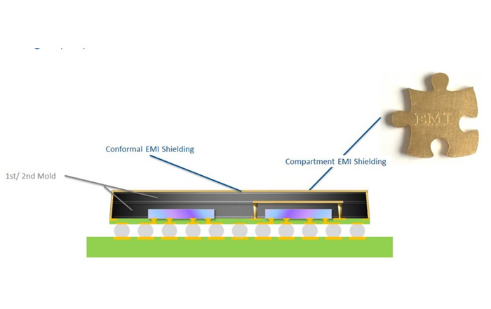
EMI shielding of IC packages and System-in-Packages (SiP)
-
EMI shielding of complete IC packages or individual areas within a System-in-Package or individual dies inside a Multi-Chip-Module is a very challenging task in terms of equipment investment, process flow, shielding reliability, production yield or design flexibility and size requirement.
AMP is offering a selection of benefits, when compared to PVD sputtering, metal lid soldering or copper paste printing.
- Low equipment investment cost and thus fast amortization
- Equipment can be used for a multitude of other novel packaging applications, like Antenna-on/in-Package, too
- Reliable shielding layer formation on the package's/SiP's sidewalls, no peel-off or flaking
- Simplifies the singulation process, as the EMC has been removed from the dicing streets, for the sidewall activation/ metalization
- Offers the highest resolution and selectivity for conformal and compartment shielding
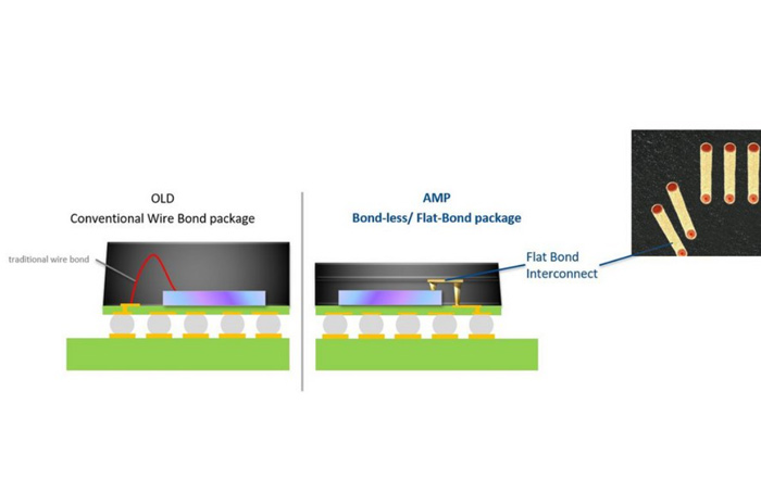
Bondless Multi-Chip Modules (MCM)
-
Active Mold Packaging interconnects dies and substrates by using the Epoxy Mold Compound, easily exceeding the resolution, pitch and yield of traditional wire-bonding (WB).
Interconnecting multiple dies with each other and with the substrate or leadframe, can result in wire bonds crossing over each other. Apart from the very challenging wire bonding task, this can lead to wire sweeping during encapsulation and prevents the use of compression molding.
Active Mold Packaging (AMP) Flat-Bond Interconnects, can replace wire bonding (WB) in all packages that make use of an Epoxy Mold Compound for encapsulation.
Flat-Bonds are offering a selection of benefits, when compared to WB.
- 50% shorter signal path lengths, lead to lower power consumption and higher RF performance
- Pitch reduction to 100 µm and a zero mm bending radius, reduces package footprint and height
- Solid, immovable connection, prevent wire-sweeping and enables compression molding
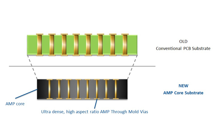
CTE Matching IC Substrate
-
Active Mold Packaging enables the use of the Epoxy Mold Compound as a mid-range L/S package substrate, alleviating the thermal stress between the semiconductor die and the copper components inside a package.
IC Packaging and SiP manufacturing require the use of many different materials. This is posing some serious challenge for the designers and packaging houses, in terms of thermally induced stress and subsequent productions yield and lifetime of the device.
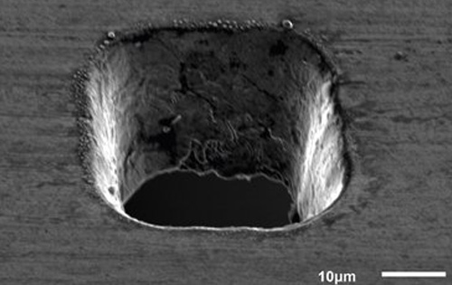
Active Mold Packaging (AMP) is a potent mean to reduce this specific complexity. It can be used as a substrate material that alleviates the different coefficients of thermal expansion (CTE) of the semiconductor die and all metallic elements inside a package. Additionally AMP is a mid-range interconnect technology with Line and Space (L/S) of 25 µm each and high-aspect ratio true Through Mold Via (TMV) formation of up to 1:10. Seen from a vantage point AMP is a strong alternative to organic substrates (FR4), for the formation of redistribution layers and can play its role even in fan-out Wafer and Panel Level Packaging (fo-WLP/ fo-PLP)
AMP is offering a selection of benefits, when compared to traditional package integrated antenna technologies.
- 20% reduced footprint, due to smaller vias and via pads
- high true TMV aspect ratio of 1:10
- better CTE match and alleviating CTE mismatches between the die and copper
- limited topography due to embedded conductors, landing- and via-pads
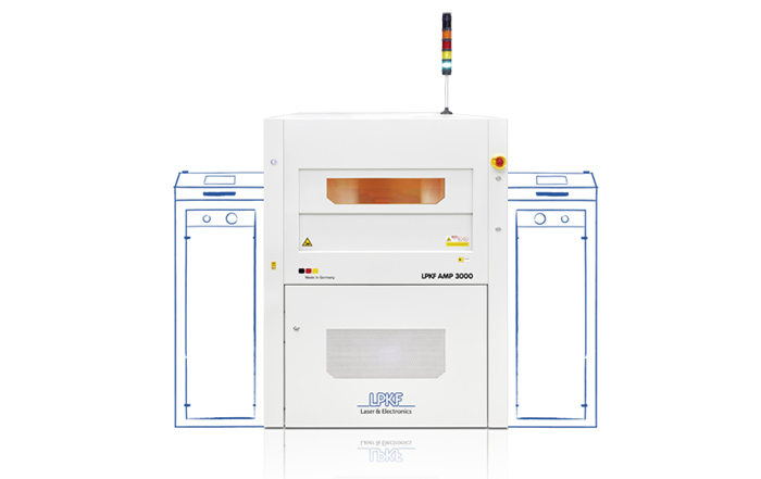
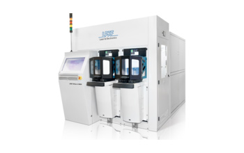
LPKF AMP 3000
-
The one laser tool to simplify your back-end manufacturing processes!
- Zero-Touch Environment
Your pathway into a Zero-Touch production environment, which increases production output and helps reducing waste. - End-to-End Traceability
The SECS/GEM compatible end-to-end traceability strengthens your customer's confidence in your products. - Made in Germany
The AMP 3000. Your above-average Back-end manufacturing turn-key solution Made in Germany. - Adaptive Die Patterning
Doubles the overall process accuracy and reliably increases your First Pass Yield percentage.
Technical Details
- Maximum Working Area: 300 x 100 mm
- Overall Positional Accuracy: ± 20 µm @ cpk 1.33
- Dimension (WxHxD): 1 050 x 2 120 mm* x 2 000 mm
- Weight: < 1 400 kg
- Power Consumption: < 5 500 Wh (< 5 000 VA)
- Handler: fully automated push-pull or roller-guided strip transport, for up to 4 magazines
- Zero-Touch Environment
Laser Depaneling
-
Contact-free process for separating Printed Cirucuit Boards
Laser Depaneling is one of the most innovative processes to separate printed circuit boards (PCBs) out of the panel. With traditional depaneling methods, assembled PCBs are cut out of the panel using a mechanical separation process. In the case of Laser Depaneling, the depanelization process is performed using a focused laser beam that ablates the material layer by layer. The laser process - especially in case of LPKF machines - offers considerable advantages over conventional mechanical cutting processes.
CleanCut-technology by LPKF
-
100% Clean Depaneling
Maximum quality and technical purity
The innovative CleanCut-technology by LPKF guarantees an unprecedented edge quality where the material is 100% carbonization-free.The CleanCut-technology is an innovative process for laser cutting of printed circuit boards. The result is a previously unattained technical cleanliness of the cutting edge and a high quality product. The processed cutting is100% carbonization-free. To achieve this technical cleanliness, LPKF machines do not require an additional cleaning step which would extend the processing time.
Overall, the probability of failure of processed PCBs can be significantly reduced by the clean and dust-free cutting edges and components.
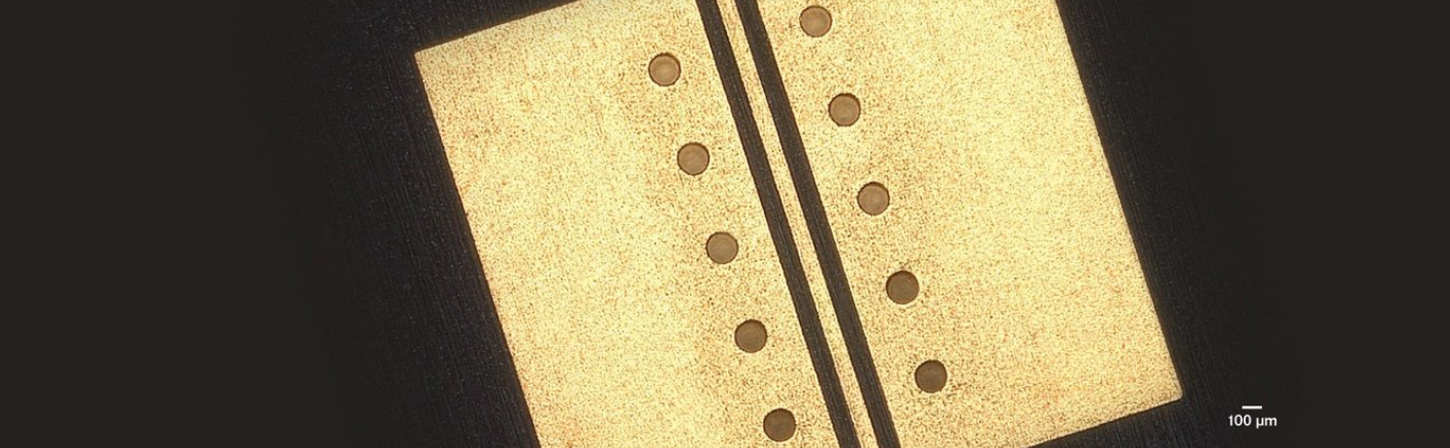
Laser Depaneling of ceramic circuit boards
-
With laser depaneling systems by LPKF printed circuit boards made of ceramic materials can be processed in addition to a wide range of other materials. The cutting edges are produced technically clean, highly precise and cost-efficient.
Laser cutting of ceramic PCBs
In contrast to conventional mechanical cutting processes of PCBs, laser depaneling allows ceramic materials to be processed easily and wear-free. The problem of extremely hih hardness is not a problem with non-contact ablation process of the laser.
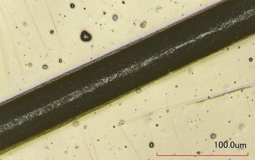
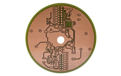
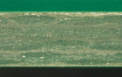
Ceramics made of aluminium oxide (see picture) can be cut technically clean at high speed even in material thicknesses of several hundred micrometers. Low (LTCC) and high (HTCC) fired ceramics can be both processed.
The laser also cuts different layouts of ceramic printed circuit boards - such as those with copper layers applied on one or both sides - technically clean and highly efficient.
The individual requirements of the different ceramic materials can be taken into account in the parameter selection of the laser processing. In this way, highly sensitive materials can be processed gently and ceramic breakage can be avoided.
Automated cutting of printed cicuit boards and panels with lasers
-
Compact, flexible and cost-efficient
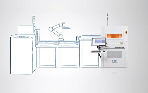
Laser depaneling systems from LPKF integrate seamlessly into existing and new production environments as well as Manufacturing Execution Systems (MES). The machines are specially designed for increasing automation and the requirements of industry 4.0.
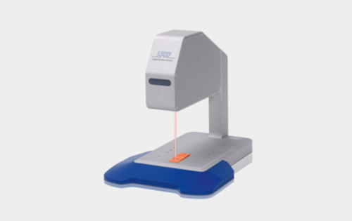
Laser induced deep etching (LIDE)
-
Deep Micro-Structures in Glass
No special glass required, no chipping, no micro cracks
The LIDE technology (Laser Induced Deep Etching) developed by LPKF is a new enabling technology for a wide range of applications in microsystems technology. The needs of end customers and their business models are as varied as the applications. We aim to offer all potential LIDE customers the most easy, barrier-free access to the technology. Our customers therefore benefit from access to production service solutions as well as from equipment solutions for selected applications and manufacturing environments.You are convinced that deep microstructures in glass can help you make your products better and would like to integrate the LIDE technology into your manufacturing process chain?
We can help you and offer special laser machines for different production environments:- Cover glass processing
- Semiconductor manufacturing
Production services
-
Do you work for a "Fab Less" company or an OEM who does not want to deal with the integration of a new, multi-stage manufacturing process?
Then our production service offer is the right choice for you. With the Vitrion-Precision-Glass-Processing-Service you determine the design of the glass components and we take care of manufacturing them economically and based on our LIDE process.
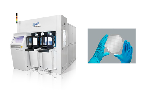
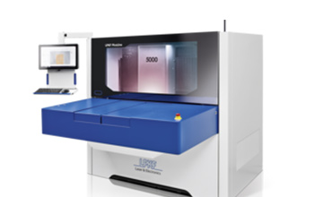
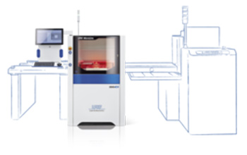
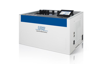
Vitrion S 5000
-
LIDE Production System for the Semiconductor Industry
Available wafer formats: 100 mm/150 mm, 200 mm/300 mm
The Vitrion S 5000 system is the production system solution for today's and future packaging and semiconductor applications with the LIDE process. The high-performance laser system processes glass wafers with unparalleled precision and speed and without causing any defects in the glass: Perfect quality for the production of through glass vias, for embedding solutions, capping wafers and advanced packaging solutions.Key specifications at a glance
- Glass wafer thickness: 0.3 to 3 mm
- Bridge tool: 150/200 mm wafer or 200/300 mm wafer
- EFEM: Two standard FOUPs
- Compatible with flat/notch wafers
- SECS/GEM for simple integration and configuration
- SEMI E84
- System dimensions (WxHxD): 1800 x 2200 x 3000 mm
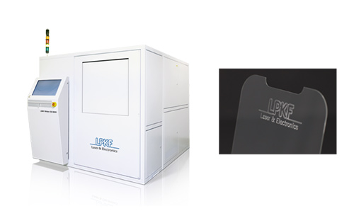
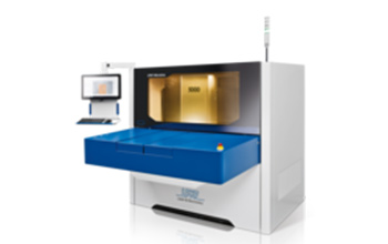
Vitrion CG 5000
-
Cover Glass Processing on a New Level
No stress, no micro cracks, no chipping -- surface defects are a thing of the past.
Display cover glasses have become an integral part of our modern life. As an essential interface to the end customer, high demands are placed on cover glasses. Conventional, mechanical processing methods inherently reach their limits. Stress, microcracks and chipping limit the resistance of the cover glasses. New requirements such as the integration of micro-holes or the folding of cover glasses cannot be implemented at all. Based on our unique LIDE technology, the Vitrion CG5000 sets new standards in coverglass processing.Applications
- Break-proof edges for cover glasses
In contrast to conventional methods of cutting cover glass for mobile handheld device applications, the LIDE process provides absolutely crack- and break-proof edges. Almost any shape of holes and break-outs can be produced, even with the smallest radii. Complex grinding and polishing steps to reduce the risk of breakage are no longer necessary. The dimensional tolerances for the mounting of the glasses can be ensured without any further processing steps. This applies both to "pencil cuts" or "C cuts" and chamfer cuts. - Production of foldable displays
With LIDE it is possible to make display glasses locally bendable by surface defect free micro cuts. This provides a solution for the use of glass in folding displays for smartphones and other mobile devices. The advantages of glass surfaces as an interface to the user can now also be applied to foldable displays. The LIDE laser system Vitrion CG 5000 impresses with its exceptionally high yield and productivity.
Key specifications at a glance
- Supported blank format: <300x300 mm
- Glass thickness: 0.3 mm up to 1 mm
- Automated glass handling with customer-specific holders
- Prepared for integration into Manufacturing Execution Systems (MES)
- System dimensions (WxHxD): 1800 x 2000 x 3100 mm
- Break-proof edges for cover glasses
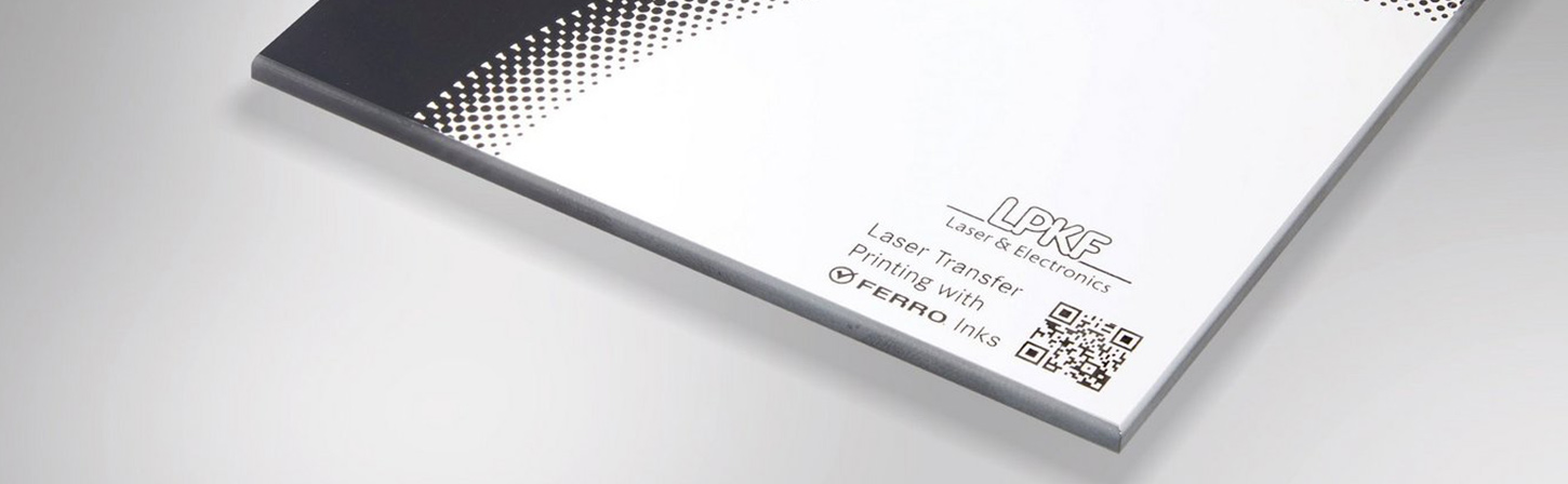
Laser Transfer Printing (LTP)
-
New Options for Automotive and Transportation Glass Printing
Laser Transfer Printing (LTP)
LPKF Laser Transfer Printing is a laser-based solution for digital printing with ceramic pigments. Ceramic colors can be transferred to flat glass with previously unknown precision.Learn more about this unique technology, applications and solutions on the special LTP-website. We are happy to get in contact with you.
Micromachining Services
-
LaserMicronics
Under the LaserMicronics brand, LPKF offers laser micromachining services. The range of services extends from feasibility studies through prototype production to series production. Specialised application engineers use the leading LPKF laser technology and ensure technically superior and high-quality products as well as cost-effective production.
-